NIC overview

NIC is network interface controller, hardware component, that connects a device to computer network.
This controllers used for connecting a device (such as computer, board (rpi/banan), phone) to networks, like LAN. It can connects to PCI, ISA, USB or be build-it to some chip (for example in Motherboard or some SoC).
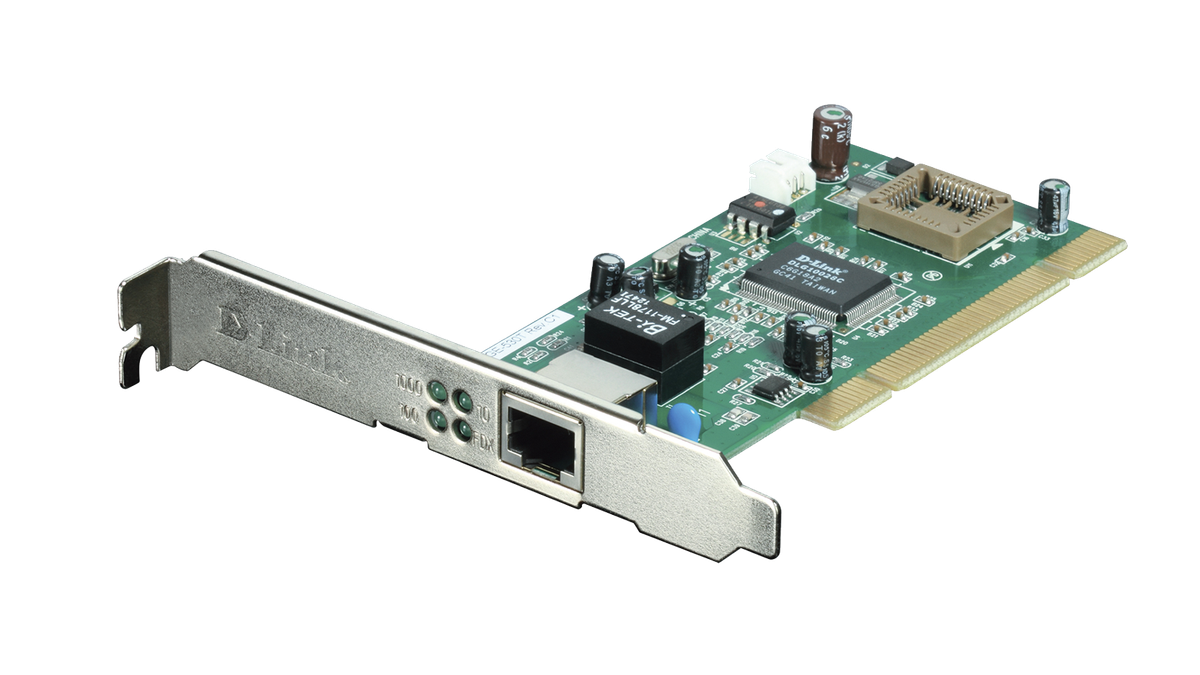
Now i want to describe main characteristics of this controller (with example of very popular Realtk 8168)
How NIC is define that connection exists
Autonegotiation
Autonegotiation is mechanism (and set of procedures) used by Ethernet (over twisted pair) to choose common transmission parametrs (between two connected devices, for example between nic and switch port) such as speed, duplex mode, flow control.
Via this process devices share their capabilities of these parametrs and then choose the highest-perfomance modes, they both support.
Autonegotiation is defined in IEEE 802.3 clause 28 (section 2).
Autonegotiation runs first, before any single data frames is exchanged.
Autonegotiation uses special pulses, called FLP (fast link pulse), it based on NLP (normal link pulses), that used by 10BASE-T for establish link integrity(??).
In FLP, controller send 17 to 33 pulses (with 125 nanoseconds delay between) in one frame. time between frames is 16 +- 8 ms (like in NLP, for supports old 10BASE-T devices to save LINK TEST PASS state).
TODO: describe why it can be 33 pulses
TODO: add pictures from wiki
What's in one (16 bit) frame:
0-4: indicates which standard is used between IEEE 802.2 and IEEE 802.9
5-12: technology ability field:
bit 0: device supports 10BASE-T
bit 1: device supports 10BASE-T in full duplex
bit 2: device supports 100BASE-TX
bit 3: device supports 100BASE-TX in full duplex
bit 4: device supports 100BASE-T4
bit 5: device supports pause frame
bit 6: device supports asymmetric pause for full duplex
bit 7: reserved
13: remote fault - set to one when the device is detecting a link failure
14: acknowledgement – the device sets this to one to indicate the correct reception of the base link code word from the other party; this is detected by the reception of at least three identical base code words. Upon receiving these three identical copies, the device sends a link code word with the acknowledge bit set to one from six times to eight times.
15: next page – used to indicate the intention of sending other link code words after the base link code word (It needed for example for gigabit negotiation, because it requires more pages)
autonegotiation phases
- Both sides transmit FLPs with ACK(14bit)=0.
- After recieving 3 FLP bursts (with ignoring of Ack bit), device goes to Acknowledge Detect and sets Ack=1.
- After 3 more FLPs with Ack=1, device enters Complete Acknowledge and trasmits 6-8 final FLF. In this phase, devices are choose highest common denominator (corresponding on base table (1000BASE-T FD > 1000BASE-T HD > 100BASE-TX FD ... ) or corresponding on special table, that written in PHY)
Gigabit autonegotiation
1000BASE-T add some complexity to autonegotiation, because it needs master/slave clock resolution - one PHY generates the 125Mhz transmit clock, while other PHY gets it.
for 1000BASE-T devices still sends basic packages, but have another two pages.
The additional pages are of two kinds: message and unformatted pages. These pages are still 16-bit words (same as basic pages), first eleven bits presents data, when other bits presents kind of page (message or unformatted). The last bit of each page indicates the presence of an additional page.
The message page contains:
half duplex capability
whether the device is single port or multiport
whether master/slave is manually configured or not
whether the device is manually configured as master or slave
The unformatted page contain a 10-bit word, called a master-slave seed value (for what??).
Old parallel detection fallback
Fiber connection
RTL 8168 example
RTL8168 used next registers for autonegotiation:
PHYAR: PHY Acess (offset 0060) - register, that has current state of link, speed mode, duplex mode and flow control
BMCR reg (address 0) - speed, autonegotiation enabling
BMSR reg (address 1) - read only values with capability for speed and duplex modes
ANAR reg (address 4) - local adverstisment (todo: for what?)
ANLPAR reg (address 5) - partner's advertisment (todo: for what?)
GBCR and GBSR (address 9 and 10) - gigabit specific things
Half-duplex
Half-duplex Ethernet uses CSMA/CD (Carries Sense Multiple Access with Collision Detection) is a MAC (media access control) method, where device listening channel before transmitting, detect collisions (when two or more devices are transmitting at one time) by monitoring voltage thresholds, sends a 32-bit signal on collision, then backs off using random time of waiting (from 0 to 2^n-1 slot times, where n is attempt count, max to 10), and after waiting tried to transmit again.
Main ideas of CSMA/CD
- CS - Carries Sense - device, that want to transmit, first is check line for free (have it or not other frequencies from other devices)
- Multiple Access - all devices have same rights on the line
- Collision Detection - if two devices are transmit at one time, collision is detected
- Actions on CD - device send 32-bit "jam" signal to notify others and start wait
- Maximum wating is 10-16, after maximum is reaching, device is stopped transmitting frame
Full-duplex
full-duplex of coures haven't any collisions.
RTL8168 supports both modes at 10/100Mbps but practiaclly operates full-duplex exclusively at gigabit. (TODO: rtl8168 have not csma/cd?).
Also standard (IEEE 802.3ab) defines half-duplex gigabit, but technically noone hardware implements it - carries extension to 512 bytes (4096 bit times) (TODO: what is it?) would make it absurdly ineffiecent.
Ethernet flow control
is a mechanism for temporarily stopping the transmission of data. The goal of this is to avoid packet loss.
A sending station may be transmitting data faster than the other side can accept it. Using flow control can fix this problem, via stop transmitting.
This mechanism is using special pause frames.
Pause frame
Overhelmed node can send a pause frame, which halts the transmission of the sender for a specified period of time. The frame format is next: destination MAC is reserved (01-80-C2-00-00-01 multicast), source - sender MAC, EtherType is 0x8808 (MAC control), opcode 0x0001 (Pause), followed by a 2-byte pause_time in units of 512-bit-time quanta. At 1 GBps, one quantum is 512 ns; the maximum value is 0xFFFF (33.55ms).
New PAUSE frame replaces any active timer and PAUSE th time=0 resumes immediately.
pause frame capability
is advertised during auto-negotiation via pause frame bit(A5) and symmetric/assymetric pause bit(A6). Ther is 4 combinations: either bit = no PAUSE; A5 only = symmetric (both send and honor); A6 only = asymmetric toward partner (send only, won't honor received); both = full support.
rtl8168
PHYstatus register reports about resolved tx/rx flow control state
TODO: add other registers
PHY
PHY-layer signaling
Or how it works on physical level.
https://en.wikipedia.org/wiki/Line_code
10BASE-T
uses Manchester encoding (Phase encoding).
Each bit occupies a 100ns period with a mandatory transition at the midpoint: high-> low for 0, low->high for 1. Signal levels are 2.5V differential.The spectral content ranges from 5 MHz (alternating 0-1) to 10 MHz (all-same bits), requiring only Category 3 cable (16 MHz bandwidth). Two pairs are used: pins 1,2 for Tx and pins 3,6 for Rx. Link integrity is maintained via Normal Link Pulses — 100 ns positive pulses every ~16 ms.
100BASE-T
First, 4B/5B mapping converts each 4-bit nibble to a 5-bit code at 125 Mbaud, with codes chosen for maximum transitions and DC balance (25% overhead). Special J/K/T/R/I control symbols handle framing. Next, LFSR scrambling flattens the spectrum for EMI compliance, followed by NRZI encoding (1 = transition, 0 = no change). Finally, MLT-3 converts to three voltage levels (−1V, 0V, +1V differential) cycling through 0→+1→0→−1→0. A complete MLT-3 cycle requires 4 binary ones, so the maximum fundamental frequency is 125 MHz/4 = 31.25 MHz — well within Category 5's 100 MHz specification. Manchester encoding at 100 Mbps would need 200 MHz bandwidth, which is why this elaborate chain exists. (TODO: review)
Also there is 100BASE-T4 (or T1, that created for automobiles), that use PAM-3
And 100BASE-T2(very rare to use), that used PAM5.
1000BASE-T
It transmits simultaneously on all four twisted pairs, each pair carrying full-duplex bidirectional data at 125 Mbaud using PAM-5 (Pulse Amplitude Modulation with 5 levels: −2, −1, 0, +1, +2). Unh Each symbol encodes 2 data bits (4 of 5 levels carry data; the 5th provides Forward Error Correction). The math: 125 Msymbols/sec × 4 pairs × 2 bits/symbol = 1000 Mbps.
The encoding uses 8B1Q4: 8 input bits map to one group of 4 quinary (5-level) symbols across the four pairs. With 5⁴ = 625 possible 4D patterns but only 2⁸ = 256 data values needed, the redundancy enables Trellis Coded Modulation — an 8-state 4D convolutional code where a 9th bit from a convolutional encoder selects symbol mappings that maximize Euclidean distance between valid sequences. This provides approximately 6 dB coding gain, exactly compensating for the 6 dB SNR penalty of going from 3 to 5 voltage levels. A Viterbi decoder at the receiver performs maximum-likelihood sequence estimation.
RTL8168 PHY DSP (Digital Signal Processing)
runs five concurrent signal processing algos withit each 8ns symbol period:
Adaptive equalization: A Feed-Forward Equalizer (FFE) compensates frequency-dependent cable attenuation, while a Decision Feedback Equalizer (DFE) cancels post-cursor intersymbol interference
Echo cancellation: Each pair carries simultaneous Tx and Rx; the local transmit signal leaks into the local receiver through the hybrid transformer. Adaptive filters (hundreds of taps) model the echo path and subtract the estimated echo in real-time
NEXT cancellation: Near-End Crosstalk from the three adjacent local transmitters on the other pairs, cancelled using 3 adaptive cancellers per receiver (the local transmitted symbols are known)
FEXT cancellation: Far-End Crosstalk from the three remote transmitters, harder than NEXT because remote symbols are initially unknown
Baseline wander correction: AC coupling through transformers removes DC; low-frequency patterns cause baseline drift that the DSP corrects
MDI & MDI-X & AUTO MDI-X
Medium Dependent Interface and Medium Dependent Interface with Crossover
As we know, there is two types of cables: straigt and crossover. (https://en.wikipedia.org/wiki/Ethernet_crossover_cable), so because of need we nood to define what cable are connected.
MDI is straight cable MDI-X is crossover. (type also depends on From/To connection)
But all modern devices are uses auto MDI-X, that can define type of cable automaticaly.
RTL8168 PHY AUTO MDI-X
For 10/100M, the standard MDI pinout places Tx on pins 1,2 and Rx on 3,6; MDI-X reverses this. The RTL8168's PHY uses a pseudo-random number generator to pick an initial configuration, attempts auto-negotiation, and swaps if no link is established. Resolution completes within 500 ms. For 1000BASE-T, where all four pairs are bidirectional, the PHY additionally performs pair swap detection (handling miswired pair-to-channel mappings), polarity correction (detecting and digitally inverting reversed conductors within a pair), and skew correction (deskew buffers align all four pairs within the IEEE 802.3ab maximum tolerance of 50 ns).
MTU
Maximum transmission unit - the size of largest PDU (protocol data unit) that can be transmitted in a single transaction.
1500 bytes legacy
The 1500-byte MTU is a 1980s compromise driven by three constraints: CSMA/CD timing at 10 Mbps (larger frames monopolize the shared medium), buffer memory costs (early NICs needed SRAM buffers ≥ max frame size, and 1536 bytes was power-of-2 friendly), and Manchester clock drift (long frames risked bit misalignment). IEEE 802.3 (1983) standardized 1518 bytes maximum frame size (14 header + 1500 payload + 4 FCS), cementing this limit.
On the wire, every frame carries overhead: 7-byte preamble + 1-byte SFD + 14-byte header + payload + 4-byte FCS + 12-byte inter-frame gap = 38 bytes of non-payload overhead.
At 1 Gbps with 1500-byte MTU, the line can have 81,274 frames per second. With 9000-byte jumbo frames, this drops to 13,888 frames per second - a 5.9× reduction in per-packet processing overhead (interrupts, descriptors, DMA transactions, protocol headers).
packages with vlan
packages with vlan tag have additional 4-byte tag. Because of it IEEE802.3ac extended the maximum frame size to 1522 bytes for this purpose.
jumbo frames
To avoid this limit was created jumbo frames (but they are not stanardtized by IEEE).
When you change mtu, you technically add jumbo frames and increase size of package to 9000bytes.
jumbo in "end-to-end support", every device in chain must support the same MTU size. If any hop has a lower MTU, frames get either fragmented (IPv4 with DF=0) or dropped with ICMP "Fragmented Needed" (IPv4 with DF=1) or "Packet Too Big" (IPv6)
jumbo frames on realtek
The RTL8168 family's jumbo frame support varies by silicon revision. The original RTL8168B (MAC versions 11–20) supports only ~4 KB jumbo frames. Later revisions improved: RTL8168C handles ~6 KB, and RTL8168D onward (MAC version 25+) supports the full ~9 KB. The Linux r8169 driver defines these limits precisely:
JUMBO_9K = (9 × 1024 − VLAN_ETH_HLEN − ETH_FCS_LEN). A significant caveat: on many RTL8168 variants, Tx hardware checksum offload is disabled when jumbo frames are enabled (the kernel logs "tx checksumming: ko"), forcing the CPU to calculate checksums for the larger frames and partially offsetting the savings from fewer packets.
VLAN
Checksum
IP, TCP and UDP have checksums. All of them uses same algo: sum of all 16-bit WORDs (including header and text) with audo-add zeroes in case of not an odd number of header + text octets.
Computing this for a 1460-byte TCP segment requires summing ~730 16-bit words. At 1Gbps with 81000 packets per second, the cpu must performs 60 million 16-bit ADD per second only for checksum calculations.
Checksum offload for RTL8168
RTL8168 try to offload it in both directions.
For Tx checksum offload, driver sets protocol-specific bits in the Tx descriptor's command DWORD: bit 18(IPCS) for IP header checksum, but 16(TCPCS) for TCP, but 17(UDPCS) for UDP. The driver pre-seeds the checksum field with the pseudo-header sum, rtl8168 computes the remainder over the actual data nad writes the funal checksum.
For Rx checksum offload (that enabled via C+ Register), controller verifies incoming checksums and reports pass/fail status bits in the Rx descriptor, allowing the kernel to skip verification.
TCP Segmentation offload (TSO)
or Large Send Offload (LSO)
Problem
When an application called send() syscall, it might send a buffer up to 64KB of data. TCP needs to deliver it all, but can't send it in single frame, because of MTU(that equal 1500 bytes).
TCP has a palametr called MSS (Maximum Segment Size) , which is MTU minus IP header(20 bytes) and minus TCP header(20 bytes min), sy typicall 1460 bytes.
And for 64Kb of data, system must send around 45 full packages (generate TCP header, generate IP header, calc TCP checksums, allocate sk_buff, fill a DMA descriptors and write registers of NIC).
The above takes time, a lot of time.
How TSO can solve it
With TSO, kernel does listed once for the entire 64KB. It build a single TCP header, one IP header and attaches the full 64KB payload.
What it does:
- Segments the data(64 Kb buffer) into MSS-sized packets
- Replicates the header template for each segment
- Adjusts TCP sequence numbers (incrementing by MSS)
- Increments IPv4 ID field
- Update IP Total Length
- Recalc IP and TCP checksums per each segment
- Sets FIN/PSH only for last segment, CWR only for first
We still have 45 packages, but we don't need useless calculations, and it can save around 30-50% of cpu time.
How it works on RTL8168
TSO is activated via the LGSEN bit in the Tx descriptor. When set, lower bits encode the MSS value.
The MTPS register (offset 00ech) controls maximum TSO packet size in 128-byte units.
Generic Segmentation Offload(GSO)
Is software-only solution.
It creates the same large packets but segments them in kernel before handing them to NIC driver. It usefull in cases, where TSO in unavailable.
Generic Recieve Offload (GRO)
Same as TSO but for recieving.
The stack processes each of those 45 incoming segments individially.
GRO coalesces consecutive TCP segments with sequential sequence numbers back into a single large buffer before passing it up the stack, reversing the segmentation
Receive Side Scaling (RSS)
In two words, RSS distributes incomping packets across multiple CPU cores using a hash-based queue assigment mechanism.
The controller parses packet header, extract from it source/dest IP and TCP/UDP ports, computes a Toeplits hash(TODO: describe it) (via shift register + XOR gate impl), then indexes into a 128-entry indirection table mapping has values to receive queues. Each queue has own MSI-X interrupt vector affinity-mapped to a specific CPU core (we can see it in /proc/interrupts).
Unfortunetly RTL8168 hasn't RSS, because of:
- It has only one Rx descriptor ring (base address at RDSAR)
- RTL8168 supports only MSI vector, not MSI-X (about pci MSI vectors i want to write another article, or maybe article about interrupts in general). In two words, MSI-X unlike MSI uses table in BAR memory space, and NIC can use this table for create per-queue interrupt vectors.
- No hash hardware, it can't calc Toeplits hash
- 2004 was start of dual-core CPU era and because of it multi-queue was not neccesary.
Receive Packet Steering (RPS)
Linux provides software alternative, RPS performs hash-based packet steering in the kernel using inter-processor interrupts, and RFS (Receive Flow Steering) steers packets to the CPU where the consuming application runs.
How RPS works
With RPS all packets arrive on a single Rx queue and get processed initialy by whatever single core handles that queue's interrupt.
But during the NAPI poll, before passing the packet up the stack, the kernel computes a software hash over the same 4-tuple (source/dest IP and TCP/UDP ports) via jhash (or similar), looks up an indirection table (the rps_cpus bitmap configured via sysfs (for example in /sys/class/net/eth0/queues/rx-0/rps_cpus )), and then enqueues the sk_buff onto the target core's backlog queue vi an IPI(Inter-process interrupt).
So with rps, core 0 handles the interrupt and NAPI poll (DMA, processing of descriptors, sk_buff allocating, hash computation), then ships the packet to core N for protocol processing (up the stack).
It's more slower than RSS, but better than nothing.
How RFS works
RPS steers based on hash. And for example RPS will send packet to core 1, but application, that consume this data, run on core 5. core 1 already have data in core's cache, but core 5 is need it and want to get it from core 1. And we get cross-core cache miss.
RFS maintains a flow-to-CPU mapping table (rps_sock_flow_table) that records which CPU core last run application. When application calls recvmsg() or recv(), kernel updates this table entry: "flow with hash X was last consumed by a thread on core 5". Then when RPS is about to steer the next packet on that flotw, it checks the RFS table and steers packet to core 5.
Configured via:
echo 32768 > /proc/sys/net/core/rps_sock_flow_entries (global flow table size)
echo 2048 > /sys/class/net/eth0/queues/rx-0/rps_flow_cnt (per-queue table size)
Interrupt
PCI Express legacy interrupt emulation
PCIe doesn't have any physical interrupt pins, but it emulates the 4 physical interrupt pins of PCI via dedicated PCIe Messages (ASSERT_INTA and DEASSERT_INTC).
Being message-based interrupt, this mechanism provides advantages of PCI layer MSI mechanism: the 4 virtual pins per device are no longer shared on the bus (but PCIe controllers can still compine legacy interrupts internaly), and interrupt changes are defend from race conditions(maybe, not sure).
Message Signaled Interrupts (MSI)
MSIdeliver interrupts as PCIe Memory Write TLPs (4-byte payload) to LAPIC(on x86) address.
No sharing. No race condition. PCIe ordering rules guarantee that an MSI Memory Write cannot pass preceding DMA MWr TLPs, so when MSI arrives, all pior DMA writes are complete.
Wikipedia said, that MSI reduced the latency of interrupts of almest three times compared to basic I/O APIC delivery.
MSI can have 1,2,4,8,16,32 interrupts vectors.
RTL uses it. RTL8168 has only one MSI vector
MSI-X
MSI-X provide opportunity to have up to 2048 interrupt vectors. Each with its own entry it BAR-based table (16 bytes per entry: address low, address high, data, vector control mask bit). Per-vector masking and pending bit Array track masked interrupts.
Interrupt coalescing
Basicly 1 Gbps with minimal 64-byte frame will generates ~1.5 Million of interrupts per second. It can consume whole CPU core. Interrupt coalesing fix this.
RTL8168 have IntrMitigate register (0xE2 in code, but in datasheet i didn't find it), from linux driver:
/*
 * Interrupt coalescing
 *
 * > 1 - the availability of the IntrMitigate (0xe2) register through the
 * >     8169, 8168 and 810x line of chipsets
 *
 * 8169, 8168, and 8136(810x) serial chipsets support it.
 *
 * > 2 - the Tx timer unit at gigabit speed
 *
 * The unit of the timer depends on both the speed and the setting of CPlusCmd
 * (0xe0) bit 1 and bit 0.
 *
 * For 8169
 * bit[1:0] \ speed        1000M           100M            10M
 * 0 0                     320ns           2.56us          40.96us
 * 0 1                     2.56us          20.48us         327.7us
 * 1 0                     5.12us          40.96us         655.4us
 * 1 1                     10.24us         81.92us         1.31ms
 *
 * For the other
 * bit[1:0] \ speed        1000M           100M            10M
 * 0 0                     5us             2.56us          40.96us
 * 0 1                     40us            20.48us         327.7us
 * 1 0                     80us            40.96us         655.4us
 * 1 1                     160us           81.92us         1.31ms
 */
But because of interactions with PCI ASPM, hardware coalescing disabled by default.
Instead of it, kernel use NAPI. When kernel get hardware interrupt, ISR disables NIC interrupts (write zeros to IMR) and calls napi_schedule(). Next softirq handler calls the driver's poll function (rtl8169_poll), which processes up to 64 packets (napi max) from rx ring without hardware interrupts. If ring drains (if work_done < budget), interrupts are re-enabled, otherwise (if budget is exhausted), napi reschedules another pull cycle.
Measurments domenstated, that ~1M pps generates only 17 hardware interrupts.
DMA
Without DMA, CPU will manually copy every byte from NIC to RAM (and otherwise). It will eat all CPU core.
With DMA, CPU just writes pointer to NIC's register. And next NIC will copy data to this memory register without using CPU.
RTL8168
is PCIe bus master. After Bus Master Enable bit (bit 2 of PCI Command Register) is set, it indepentedly issues Memory Read and Memory Write TLPs to access host RAM.
Each descriptor is a 16-byte struct:
/*General view: */
struct Descriptor {
    uint32_t opts1;     // Command/status: OWN, EOR, FS, LS, length, offload flags
    uint32_t opts2;     // VLAN tag, additional checksum flags
    uint64_t addr;      // Physical buffer address (64-bit DMA capable)
};

/*RTL driver: */
struct TxDesc {
	__le32 opts1;
	__le32 opts2;
	__le64 addr;
};

struct RxDesc {
	__le32 opts1;
	__le32 opts2;
	__le64 addr;
};
RTL8168 supports up to 1024 descriptors per ring.
It has only three rings:
- RX
- Normal-Priority TX
- High-Priority TX
Linux driver support by default 256 Tx and 256 Rx descriptors per ring.
TX descriptor
opts1 bit layout:
bit 31 = OWN (1 = NIC owns)
bit 30 = EOR (End of Ring, triggers wraparound to descriptor 0)
bit 29 = FS (First Segment)
bit 28 = LS (Last Segment)
bit 27 = LGSEN (TSO enable)
bit 18 = IPCS
bit 17 = UDPCS
bit 16 = TCPCS
bits 15:0 = frame length
The Tx flow proceeds: driver fills the buffer, writes the physical address to addr, sets opts1 with OWN=1 and appropriate flags. Then writes the TxPoll register (offset 0x38) as a doorbell trigger. The NIC DMA-reads the descriptor (16-byte MRd TLP), DMA-reads the packet data (MRd → CplD TLPs), transmits from its internal Tx FIFO, then clears OWN via a MWr TLP. The driver reclaims completed descriptors in the poll function.
RX descriptor
During init stage, driver allocates buffers (~16 KB each), writes their addresses into descriptors, and sets OWN=1(buffer ready to use for NIC). When a packet arrives, NIC DMA writes packet data to the buffer (MWr TLPs), then updates the descriptor: clears OWN, writes received length, set status flags (OK checksum, VLAN tag present, multicast, error bits). If no descriptor have OWN=1 (ring exhausted), NIC asserts activate RDU interrupt and drops packets.
Scatter-gather
Scatter-gather means, than single packet can use multiple not-contiguous memory buffers.
On transmit side, this matters beacuse packet is assembled from different things: TCP header might be in one buffer, payload in second buffer, VLAN tag in other. Without gather, kernel will copy all pieces to one buffer, before send it to NIC. With gather, kernel marks first descriptor with FS=1 (first segment) pointing to header buffer, middle descriptors point to payload chunks and the last has LS=1(last segment). NIC reads them all and assemble full packet.
On receive side, kernel might want to fit packet (for example big jumbo packet) in different buffer (because this packet doesn't fit in one pre-allocated buffer). And for this NIC will send packet via multiple descritpors using FS/LS.
The core benefit of it is avoiding memory copies. Without this technology kernel will copy a lot of data to create contigious layouts.
Buffers
RTL8168 has in-chip SRAM FIFO buffers (8 Kb Tx and 16 Kb Rx). This buffers are needed for store-and-forward buffers between DMA and the wires. It prevents underrun during DMA latency spikes (for 1Gbps, 64-byte packet takes ~672ns on wire and 8KB buffer can save ~125 such packets).
The Rx FIFO Threshold (RCR register offset 0x44, bits 15:13) controls when DMA begins: configurable from 64 bytes to "no threshold" (wait for entire packet) (TODO: describe it).
About PCIe
RTL8168 uses PCIe 1.0 x1
PCIe 1.0 x1 provides 2.5 GT/s (gigatransfers per second) with 8b/10b encoding.
Afeter encoding overhead (around 20% lost), we get 250 Megabyte in second per direction. It's 2x of gigabit maximum (125 Megabyte per second).
Architecture
PCIe use standard layered packet architecture.
- Transaction Layer Packets (TLP) are the atomic units. 3 or 4 DWORD header (Fmt, Type, Length, Requester ID, Tag, byte enables); payload (0-4096 bytes); optional ECRC.
- Data link layer wraps each TLP with sequence number and LCRC for delivery with ACK/NAK.
- Physical layer handles 8b/10b encoding. LFSR scrambling (XOR with polynomial-generated stream to flatten spectral density for EMI compliance, I DON'T FUCKING UNDERSTAND WHAT IS IT, I COPY IT FROM SITE) and differential signaling.
DMA
NIC DMA operations map directly to TLP types.
Rx packets writes to host memory use posted MW TLPs (fire-and-forget, without ACK at TLP level)
Tx packets reads from host memory use non-posted MRd TLPs (with CpLD responses) - NIC must wait for data, which bounds throughput for small reads.
MSI interurpn delivery is MWr TLP (4-byte payload to LAPIC (in x86)), which PCIe ordering rules guarnatee cannot pass preceding DMA MWr TLPs.(read MSI section)
PCIe PHY
RTL8168 PCIe PHY supports lane polarity reverse (invert Tx+/Tx-) and link reverse. It good for board developing.
Power
RTL8168 has full ACPI Power Managment (states from D0 to D3cold). Controlled by PCI PM Capability register.
D0 is fully operational - all registers accessible, all power rails active
D1 and D2 are progressive sleep, with context preserved, but I/O and memory spaces are disabled.
D3hot are state, when all context are removed and keep only Vcc voltage and PME context (PME-En, PME_Status and PowerState).
D3cold removes main power entirely - only 3.3V auxiliary power remains for Wake-on_LAN.
The Power Management Control/Status Register (PMCSR) controls state transitions: bits 1:0 encode the PowerState (00=D0, 01=D1, 10=D2, 11=D3hot). Bit 15 (PME_Status) is set when the device asserts PME, cleared by writing 1. Bit 8 (PME_En) enables PME assertion. The PMC Capabilities register reports which D-states can assert PME via bits 11–15.
The RTL8168's four power supply domains (VDD3 at 3.3V, VDD1 at 1.8V, V0VDD at 2.5V analog, VDD1A for PCIe PHY) relate to power states — deeper states power down more domains. The EEDI/AUX pin serves dual purpose: during power-on, if pulled high to Vaux via a resistor, the chip detects auxiliary power and advertises D3cold PME support in the PM Capabilities register.
Wake-on-LAN
Wake-on-LAN operates through 3 mechanisms.
Magic Packet detection scans every received frame for a synchronization stream (6 bytes of 0xFF) followed by the target MAC address repeated 16 times — 102 bytes that can appear anywhere within any Ethernet frame.
Wakeup Frame detection uses programmable CRC-based pattern matching: the driver stores byte masks and CRC values for up to 4–8 patterns, and the NIC triggers a wake event when a received frame's selected bytes produce a matching CRC.
Re-LinkOk wakes on link state change (cable insert).
In D3cold, the NIC reduces to a 10 Mbps link to minimize power consumption while maintaining magic packet detection capability. When triggered, the NIC sends a PCIe PM_PME message, causing the chipset to signal the PSU for full power-up.
Maximum 3.3Vaux draw per PCI PM spec: 375 mA. (in D3cold state)
ASPM
PCIe active state PM operates independ from D-state managment.
TODO: describe it, but as i read aspm for realtek isn't good thing
EEPROM
RTL8168 requires external EEPROM chip.
The 93C46 or 93C56 (1k or 2k bit EEPROM).
Interface has next lines:
EECS - chip select
EESK - serial data clock
EEDI/Aux - input data bus / Input pin to detect if Aux.
EED0 - Output data bus
Commands begin with a start bit followed by a 2-bit opcode and address: READ (opcode 10), WRITE (01, self-timed ~5 ms), ERASE (11), and housekeeping commands EWEN/EWDS for write enable/disable.
Endurance: ~1 million erase/write cycles with 100-year data retention.
After power-on, the RTL8168 automatically reads EEPROM addresses 00h through 3Fh and loads content into internal registers.
Stored data includes the MAC address (6 bytes, loaded into IDR0–IDR5), PCI Subsystem Vendor/Device IDs (loaded into configuration space offsets 0x2C–0x2F), LED configuration, WoL defaults, PHY parameters, and a validation checksum.
Programming is possible via the 9346CR register (offset 0x50): setting EEM bits to 10 enables bit-bang mode where software directly toggles EESK/EEDI/EECS through register writes. Alternatively, the Vital Product Data capability (PCI Capability ID 0x03) provides standardized access — a 15-bit VPD Address Register with a completion Flag bit, and a 32-bit VPD Data Register for 4-byte transfers.
LED
The RTL8168's four LED outputs (LED0–LED3) are configured via the LEDS1–0 bits in the CONFIG1 register (offset 0x52), with initial values loaded from EEPROM.
Four modes are available:
Mode 00 assigns LED0=Link/Activity, LED1=Link(10M), LED2=Link(100M).
Mode 11 assigns LED0=Link/Activity, LED1=Link(10/100M), LED2=Link(1000M).
LEDs are typically active-low, directly driving LEDs through current-limiting resistors at 8–12 mA.
The Link/Activity LED stays continuously on when link is established and blinks during data traffic (30–80 ms on-period per packet burst).
PXE network boot
For PXE network boot, the RTL8168 supports an external Boot PROM up to 128 KB via a 17-bit address bus (MA[16:0]) and 8-bit data bus (MD[7:0]). The ROM begins with the standard PCI Expansion ROM header — the 0xAA55 signature at offset 0, ROM size at byte 2, and a pointer to the PCI Data Structure at offset 0x18. The PCIR structure identifies the vendor (0x10EC), device (0x8168), and code type (0x00 for x86 BIOS). The PXE boot sequence proceeds: BIOS discovers the expansion ROM via the XROMBAR register (PCI config offset 0x30), copies it to shadow RAM, and calls its initialization entry point. When selected for boot, the PXE code performs DHCP/BOOTP to obtain an IP address and TFTP server, downloads a Network Bootstrap Program, and transfers control. iPXE, the modern open-source alternative, can be burned into the ROM flash for HTTP/HTTPS boot, iSCSI SAN boot, scripting, and DNS resolution.